
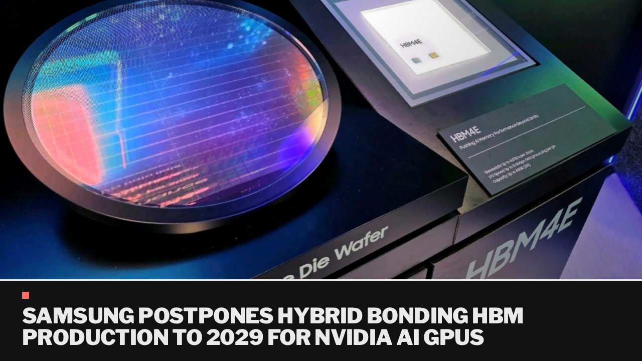
Samsung plans to begin mass production of chips using hybrid bonding technology by the end of the decade, as reported by Korean industry sources. This technology involves eliminating micro bumps in individual DRAM layers during the production of high bandwidth memory (HBM), potentially enhancing performance and reducing layer spacing.
Hybrid bonding is anticipated to be integral to the next generation of HBM, aligning with NVIDIA’s upcoming Feynman AI GPUs, which are expected to follow the Rubin Ultra chip series. The introduction of this technology may significantly advance memory performance in conjunction with these new GPUs.